Realization of Logic gates using Hardware Description Language
Realization of Logic gates
AIM: To develop the HDL Source Code for the logic gates.
Tools/Software Required:
1.
Personal Computer.
2.
Vivado 2019.2 Software
3.
Verilog/VHDL
THEORY:
AND: AND gate produces an output as
1, when all its inputs are 1; otherwise, the output is 0. This gate can have a
minimum of 2 inputs but output is always one. Its output is 0 when any input is
0.
OR: OR gate produces an output as 1,
when any or all its inputs are 1; otherwise, the output is 0. This gate can
have a minimum of 2 inputs but output is always one. Its output is 0 when all input
are0.
NOT: NOT gate produces the
complement of its input. This gate is also called an INVERTER. It always has
one input and one output. Itsoutputis0wheninputis 1andoutputis1 when input is0.
NAND: NAND gate is actually a series
of AND gate with NOT gate. If we connect the output of an AND gate to the input
of a NOT gate, this combination will work as NOT-AND or NAND gate. Its output
is 1 when any or all inputs are 0, otherwise output is 1.
NOR: NOR gate is actually a series
of OR gate with NOT gate. If we connect the output of an OR gate to the input
of a NOT gate, this combination will work as NOT-OR or NOR gate. Its output is
0 when any or all inputs are1, otherwise output is 1.
XOR:X-OR gate produces an output as
1, when number of 1’s at its inputs is odd,
otherwise output is 0. It has two inputs and one output.
Procedure:
·
Click on Vivado2017.2 icon.A
window is opened.
·
Click on File →New Project
→Press Next →Give the Project name and Project Location →Press Next →Choose
Project Type as RTL Project →Press Next →
·
Create File →File Type: VHDL/Verilog
File Name → Filename →Press Next → Press Next → Press Next →Finish.
·
Write the module definition by
giving input ports and output ports
→Press Ok.
·
Two workspaces are opened with
names Project Manager and Flow Navigator
·
In Project Manager →Click on
Sources →Design Sources →File →A window is opened
with File name. Write the Program in the File →Click on Save.
·
In Flow Navigator →Click on Simulation
→Run Simulation →Run Behavioural Simulation →A window is opened with name
“untitled1” →Force Constants →Run for 100 µs. Observe the simulation results
for various combinations by clicking on Zoom Out.
VHDL Code for Logic Gates
library IEEE;
use
IEEE.STD_LOGIC_1164.ALL;
entity logicgates is
Port ( a,b : in
STD_LOGIC;
y0,y1,y2,y3,y4,y5,y6 :
out STD_LOGIC);
end logicgates;
architecture Behavioral
of logicgates is
begin
y0<= not a;
y1<= a and b;
y2<= a or b;
y3<= a nand b;
y4<= a nor b;
y5<= a xor b;
y6<= a xnor b;
end Behavioral;
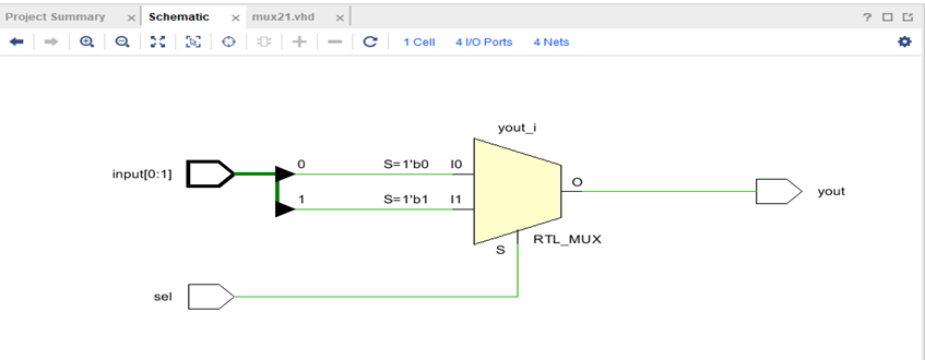
RTL Schematic for Logic
Gates


VERILOG CODE for
Logic Gates
module logic(a,b,p,q,r,s,t,u,v);
input a,b;
output p,q,r,s,t,u,v;
and(p,a,b);
or(q,a,b);
not(r,a);
nand(s,a,b);
nor(t,a,b);
xor(u,a,b);
xnor(v,a,b);
endmodule
RTL Schematic for Logic
Gates

Simulation Waveform for Logic Gates

Result:
The logic gates are simulated using
Vivado2017.2 software on an I3 Processor with 64-bit Operating System.

Comments
Post a Comment